CMOS Technology for cadence
Cadence needs a technology file to define the masks and
design rules that
are used in the fabrication process. For homework #7 we
used the MUMPS process. For hw#8 we will use the MOSIS 2um
CMOS process -- so we will have to use a different technology
file. This technology file is
/home/pp/cadusers/rconant/cmos/scmos-mems-10.tf
Whereas the MUMPS process is exclusively a MEMS process, the
MOSIS process was designed for CMOS electronics -- so the layer
names and design rules were written for electrical circuits
rather than mechanical structures.
The layers that we will use in this technology file are:
- nwell: This layer defines a well -- a region that is doped n type
for creation of a PMOS device.
- active: This defines an area where the Field Oxide is etched away.
- nselect: This selects n-type dopant for the silicon substrate.
- pselect: Similar to nselect, except it defines a p-type area.
- poly: This layer defines the location of a polysilicon line.
- metal1: The first layer of metal interconnect.
- via: The contact between metal1 and metal2.
- metal2: The second layer of metal interconnect.
- via2: The contact between metal2 and metal3.
- metal3: The third layer of metal interconnect.
- contact: Contact to the substrate.
- glass: This layer defines holes in the overglass -- the thick layer
of oxide that is used to protect the circuitry.
- pit: This is a special layer that has been added for MEMS designers.
A shape drawn on this layer will be used for every oxide etching mask --
including contact, via, via2, and glass.
To use the CMOS technology, create a library as you did before,
but choose /home/pp/cadusers/rconant/cmos/scmos-mems-10.tf
You probably won't be making electronics for this homework
-- unless you would like to make an amplifier for your
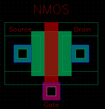
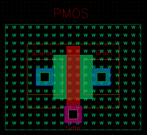
sensor -- but here are examples of MOS devices made with
the MOSIS 2um CMOS process:
NMOS:

PMOS:

Send comments to rconant


